pcb board play in the Internet of Things IoT
The Internet of Things IoT is a massive disruption of the physical world brought forth by the creation of devices that connect to IP networks, from consumer electronics like smartphones and tablets to automobiles and medical devices. IoT’s potential is even more revolutionary in industrial applications such as manufacturing, transportation and healthcare, where it can converge IT (information technology) with OT (operational technology) to streamline processes on a global scale.
IoT’s power comes from its ability to sense the physical environment, retrieve data from it and transform it into information that software algorithms can understand. In order to do this, IoT devices require a host of electronic components like sensors, radio communication modules and microcontrollers, all powered by pcb board.
To be able to function properly, IoT devices must collect data from their surroundings, send it to the cloud and then translate that information into action. To do this, they must communicate with other IoT devices and with the outside world using a variety of different connectivity options such as Wi-Fi, Bluetooth, satellite or low-power wide-area networks. Once the data is processed in the cloud, it can then trigger a response on the device, for example, sending an alert or automatically adjusting the sensor or device without user input.
What role do pcb board play in the Internet of Things IoT
As IoT devices become increasingly complex and functional, their PCBs are expected to deliver greater performance and reliability while ensuring cost competitiveness and scalability. To do this, PCB designers must rely on advanced manufacturing techniques that offer flexible production capacities and high-precision assembly processes.
In addition, IoT devices are curated to operate on battery power for extended periods of time, which increases the need for energy efficiency and power optimization in their PCBs. As such, manufacturers are implementing advanced power distribution and management systems to maximise battery life. This includes integrating low-power components, optimising board layouts and incorporating other energy-saving features.
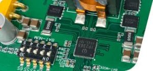
A PCB is an intricate network of copper traces, pins and other elements that are soldered together to form a circuit. In the same way that a city has streets and addresses, each pad on a PCB is identified by a silkscreen printed with a unique number. This helps PCB technicians and engineers find the component they need to solder on it, regardless of where it is on the board.
The design of IoT PCBs requires collaboration between mechanical designers and electrical engineers throughout all phases of product development, from evaluating new forms to choosing the right PCB materials and circuit board layouts for optimal functionality. To achieve this, manufacturers are leveraging advanced manufacturing techniques and automated machinery to ensure consistent quality and speed while keeping costs down. In turn, this ensures a fast turnaround from prototyping to mass production so IoT products can quickly reach consumers.