solder paste stencil play in Flexible printed circuit board
A solder paste stencil is the most important element of the surface mount technology (SMT) assembly process for flexible printed circuit boars. It facilitates the precision deposition of solder paste on the surface mount components on the PCB and ensures the quality of the final product. The importance of high-quality stencil printing cannot be overstated, as it directly influences the functionality and reliability of the assembled products.
In order to achieve accurate and consistent stencil performance, a variety of factors must be taken into consideration. These include design preparation, material selection, fabrication, and maintenance. Stencil thickness is also a critical factor, as it determines the amount and type of solder paste that can be applied to each pad on the board.
During the design preparation stage, a PCB stencil is meticulously designed based on the flexible printed circuit board PCB layout. This is done to accurately determine the precise aperture sizes and shapes for each component on the circuit board. In addition, various design specifications are also considered during this phase, including the size and placement of the surface-mount components, solder paste volume requirements, and assembly specifications.
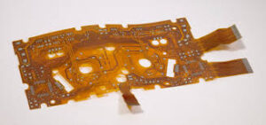
What role does a solder paste stencil play in Flexible printed circuit board
After the stencil is designed, it is then fabricated using one of several techniques, including laser cutting and chemical etching. The fabrication method chosen will influence the final stencil’s durability, precision specifications, and cost. The most commonly utilized materials for PCB stencils are stainless steel and nickel, both of which offer superior mechanical properties and longevity.
Stencil maintenance is essential for ensuring that the PCB stencil continues to function at its optimal level throughout its lifespan. This maintenance includes routine cleaning and inspection, as well as rework or replacement when necessary. Proper maintenance helps to prevent problems such as excessive solder paste build-up or bridging, which can cause defects in the finished product.
Once the stencil is cleaned and inspected, it must be dried completely to ensure that moisture residue does not interfere with the paste application process. This step is also critical for preventing misalignment between the PCB and stencil, which can have a negative impact on device function.
Finally, a metal squeegee is used to uniformly spread the solder paste over the entire stencil surface. The angle and pressure of the squeegee as well as the direction in which it is moved across the stencil surface will determine how properly the solder paste is applied to the pads on the circuit board.
Stencils can be made from a variety of materials, including Mylar and polyimide. The thickness of the stencil depends on the size and pitch of the component, with smaller components requiring thinner stencils and larger ones requiring thicker stencils. Regardless of the material used, it is vital to ensure that the stencil has an aperture opening that is 10% less than the pad size. A stencil that is too large can lead to solder paste spilling beyond the pad and onto areas of the circuit board that are not intended for it.